Transistor: Difference between revisions
imported>John R. Brews m (→Bipolar junction transistor: comma) |
imported>John R. Brews m (→MOSFET) |
||
| Line 14: | Line 14: | ||
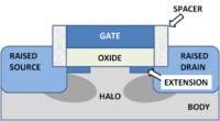
{{Image|MOSFET junction structure.PNG|right|200px|A miniaturized [[MOSFET]], like those in [[integrated circuit]]s. }} | {{Image|MOSFET junction structure.PNG|right|200px|A miniaturized [[MOSFET]], like those in [[integrated circuit]]s. }} | ||
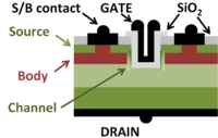
{{Image|UMOSFET.PNG|left|200px|A power MOSFET; source and body share a contact.}} | {{Image|UMOSFET.PNG|left|200px|A power MOSFET; source and body share a contact.}} | ||
The figures show two example MOSFETs. The input terminals are usually the gate and source contacts, and the output terminals at the source and drain contacts. However, as for the bipolar transistor, some circuits use different input and output contacts. For more detail see the article [[MOSFET]]. | The figures show two example MOSFETs. The input terminals are usually the gate and source contacts, and the output terminals at the source and drain contacts. In many applications, the source and body contacts are short-circuited, making a three-terminal device. However, as for the bipolar transistor, some circuits use different input and output contacts. | ||
For more detail see the article [[MOSFET]]. | |||
Revision as of 14:00, 10 June 2011
In electronics, a transistor is a semiconductor device that allows a signal at its input terminal(s) (usually a current or a voltage) to control an output signal at its output terminal(s), acting either as a switch activated by the input signal or as an amplifier for the input signal. The most common transistors are the three-terminal bipolar transistor and the four-terminal Metal-oxide-semiconductor field-effect transistor or MOSFET.
Bipolar junction transistor

A planar bipolar junction transistor as might be constructed in a integrated circuit.
A planar bipolar transistor is shown in the figure. The input terminal may be any of the three contacts and the output is connected to the other two. In a common emitter circuit, the emitter (E) is common to input and output, while the signal is applied to the base (B) and the collector (C) is part of the output circuit. Other circuit arrangements make either the collector or the base common to both the input and output.
In the figure, the labels p, n, p+, n+ refer to dopant impurities, with p referring to dopants that introduce positive charge carriers (holes) and n to dopants that introduce negative charge carriers (electrons). The superscript '+' indicates heavy doping.
For more detail see the articles bipolar transistor and semiconductor.
MOSFET
The figures show two example MOSFETs. The input terminals are usually the gate and source contacts, and the output terminals at the source and drain contacts. In many applications, the source and body contacts are short-circuited, making a three-terminal device. However, as for the bipolar transistor, some circuits use different input and output contacts.
For more detail see the article MOSFET.

