User:John R. Brews/Draft
Schottky diode
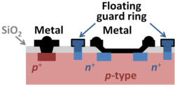
The Schottky diode is a two-terminal device consisting of conductive gate (for example, a metal) on top of a semiconductor body. A generic name for this structure is the metal-semiconductor diode or M/S diode.[1] For low voltage applications, below 200V, silicon is used, but for higher voltages (up to 3000 V or more) silicon carbide is used to extend the breakdown voltage. These voltages are achievable only when edge breakdown is avoided, which requires special attention to edge termination designs.[2] The figure shows three strategies toward increasing the edge breakdown voltage: an extension of the metal diode contact over a tapered oxide and also an n+-guard ring and a floating guard ring. These strategies are sometimes used together, but also are used separately. The substrate contact is made through an ohmic contact to the p-substrate made using a metal-to-p+ region on the surface of the diode.
Applications
The Schottky diode is used in a large variety of applications, ranging from practical devices for switching, rectification and photo-detection, to test structures for fabrication monitoring and for studies of semiconductor defects and processes.
Operation
Three different bias cases are examined: zero bias, forward bias, and reverse bias. A simplified one dimensional analysis along a line vertically through the center of the Schottky contact is used throughout. It is imagined that the p+-ohmic contact is vertically below the Schottky contact.
Zero bias
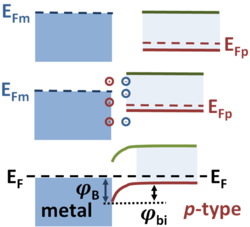
The figure shows (top) a charge-neutral, partly filled metal energy band and a charge-neutral semiconductor valence and conduction band, electrically isolated from each other. The Fermi level in the p-type semiconductor is near its valence band edge, as set by its acceptor impurity doping. (See Fermi level). The Fermi level in the metal marks the top of the filled electron energy levels in a partly filled band of the metal.
Ordinarily, the Fermi levels of different materials differ. When they are brought into electrical contact, enabling electron transfer between the materials, the work done in removing an electron from one material and placing it in the other is equal to the energy difference in the Fermi levels. Consequently, energy is released upon contact by electron transference from the material with the higher Fermi level to the material with the lower Fermi level. This charge transfer continues until the electrical charge difference means the energy gain from transfer is countered by the electrical work required against the charge difference. At this point the two Fermi levels are brought into coincidence and no further charge transfer occurs. This flat Fermi level situation (bottom panel) corresponds to thermal equilibrium, and no net current flows once equilibrium is reached.
The occurrence of charge transfer naturally means that the two materials acquire a charge. In the figure, the metal loses electrons and forms an extremely thin positive charge layer near the interface. The semiconductor gains electrons, as indicated by the bending of the valence band edge away from the Fermi level, which increases the valence band occupancy by electrons. Differently stated, the vacancies (holes) in the valence band are reduced in number, and the charge balance in the band-bending region is lost. In this depletion layer (the holes or majority carriers are depleted), the immobile negative acceptor dopant ions make this region charge negative, and this charge results in a potential according to Poisson's equation. The potential decreases with distance toward the bulk semiconductor, and at some distance (the depletion width) the bulk properties of the semiconductor are regained and the semiconductor bulk is charge neutral.
The resulting potential drop across the semiconductor depletion layer is called the Schottky barrier height, labeled φB in the figure. It is a form of contact potential.
Forward bias
If a forward bias voltage is applied VF, the Fermi level of the bulk metal EFm (in eV) is raised in energy above the bulk Fermi level in the semiconductor EFp, which lowers the Schottky barrier height to a value φB−VF. A current of holes now flows from the semiconductor to the metal (or, equivalently, of electrons from the metal to the semiconductor). Notice that the alignment of the metal Fermi level relative to the semiconductor band edges is not changed by the bias: that is fixed by the processes involved in adjusting the Fermi levels to achieve equilibrium at zero applied bias.
Reverse bias
Notes
- ↑ The term "Schottky diode" may be taken erroneously to refer to diffusion as the mechanism of operation as first proposed by Mott, Schottky and Davydov. However, the mechanism in most devices is thermionic emission, as later proposed by Bethe. See Chih-Tang Sah (1991). “§560: Metal/semiconductor diode”, Fundamentals of solid-state electronics. World Scientific, p. 474. ISBN 9810206372.
- ↑ B. Jayant Baliga (2005). “§3.2 Schottky diode edge terminations”, Silicon carbide power devices. World Scientific, pp. 44 ff. ISBN 9812566058.
http://books.google.com/books?id=FPlJQ0iO7oQC&pg=PA134&dq="Schottky+diode"&hl=en&ei=iAg6TeO7AYSasAOk67WhAw&sa=X&oi=book_result&ct=result&resnum=8&ved=0CGIQ6AEwBw#v=onepage&q="Schottky diode"&f=false


