Metal Oxide Semiconductor Field Effect Transistor
The Metal Oxide Semi-conductor Field Effect Transistor (MOSFET) is a type of FET that consists of three layers: semi-conductor (called body), oxide (working as insulator) and metal top electrode (conductor, called gate).
There are four contacts altogether: in addition to the gate and body contacts already descirbed, there are two contacts atop the body at opposite sides of the gate called source and drain. Because the transistor is symmetrical, they can swap their functions. They do not permit current flow to the body in normal operation, as they form reverse biased diodes with the body. They do allow current between source and drain upon formation (by the gate) of a surface channel at the top surface of the body, next to the insulator. The channel conductivity depends upon the voltage difference between the gate and body (Vgb). The amount of current drawn in the channel depends upon the voltage drop across it, the drain to source voltage (Vds). The channel strength also is affected by so-called "back gate bias", that is, by the body to source voltage (Vbs).
The control of the channel by the gate is similar to the formation of an inversion layer in the MOS Capacitor, which is only a two-terminal device (gate and body contacts).
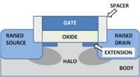
The modern MOSFET structure is shown in the figure. It is rather complex, as it is made to control a number of undesirable or parasitic effects that detract from its ideal behavior. Among these are unwanted capacitances between the gate and source and gate and drain, reduced by introduction of spacers at the sides of the gate. Another problem is high source-to-body and drain-to-body capacitance, which is reduced by raising the source and drain above the body, so the sidewall contact areas are reduced. These parasitic capacitances have to be charged and discharged between on and off conditions, and slow down device operation. Also undesired is penetration of the source and drain fields underneath the gate, which interferes with the channel formation. That effect is reduced by use of shallow junction extensions and screening halo implants, both designed to keep the source and drain fields close to their electrodes, and away from the gate.
