Semiconductor diode: Difference between revisions
imported>John R. Brews (Post new article) |
imported>John R. Brews m (→Zero bias) |
||
| Line 24: | Line 24: | ||
===Zero bias=== | ===Zero bias=== | ||
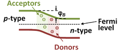
{{Image|Pn-junction zero bias.PNG|right|250px|Band-bending diagram for ''pn''-junction diode at zero applied voltage.}} | {{Image|Pn-junction zero bias.PNG|right|250px|Band-bending diagram for ''pn''-junction diode at zero applied voltage.}} | ||
As shown in the band-banding diagram at the right, when a ''p''-type and an ''n''-type region of the same semiconductor are brought into contact, the Fermi occupancy level is situated at a constant level. This level insures that in the field-free bulk on both sides of the junction the hole and electron occupancies are correct. However, a flat Fermi level requires the bands on the ''p''-type side to move higher than the corresponding bands on the ''n''-type side. Consequently, a region near the junction becomes depleted of both holes and electrons, forming an insulating region with no mobile charges. However, the absence of mobile charge means that | As shown in the band-banding diagram at the right, when a ''p''-type and an ''n''-type region of the same semiconductor are brought into contact, the Fermi occupancy level is situated at a constant level. This level insures that in the field-free bulk on both sides of the junction the hole and electron occupancies are correct. However, a flat Fermi level requires the bands on the ''p''-type side to move higher than the corresponding bands on the ''n''-type side. Consequently, a region near the junction becomes depleted of both holes and electrons, forming an insulating region with no mobile charges. However, the absence of mobile charge means that mobile charges are not present to compensate for the immobile charge contributed by the dopant ions: a negative charge on the ''p''-type side dues to acceptor dopant and as a positive charge on the ''n''-type side due to donor dopant. The dimensions of this depletion region adjust so the negative acceptor charge on the ''p''-side exactly balances the positive donor charge on the ''n''-side, so there is no electric field outside the depletion region on either side. In this band configuration no voltage is applied and no current flows through the diode. To force current through the diode a ''forward bias'' must be applied, as described next. | ||
===Forward bias=== | ===Forward bias=== | ||
Revision as of 17:55, 9 January 2011
A semiconductor diode is a two-terminal device that conducts current in only one direction, made by joining a p-type semiconducting layer to an n-type semiconducting layer.
Electrical behavior
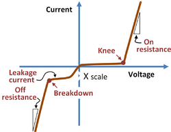
The ideal diode has zero resistance for the forward bias polarity, and infinite resistance (conducts zero current) for the reverse voltage polarity. The pn-diode is not ideal. As shown in the figure, the diode does not conduct appreciably until a nonzero knee voltage (also called the turn-on voltage) is reached. Above this voltage the slope of the current-voltage curve is not infinite (on-resistance is not zero). In the reverse direction the diode conducts a nonzero leakage current (exaggerated by a smaller scale in the figure) and at a sufficiently large reverse voltage below the breakdown voltage the current increases very rapidly with more negative reverse voltages.
Types
Semiconductor diodes come in a large variety of types:
- pn-diode: The pn junction diode consists of an n-type semiconductor joined to a p-type semiconductor.
- Zener diode: The Zener diode is a special type of pn-diode made to operate in the reverse breakdown region, and used often as a voltage regulator. The breakdown voltage in these didoes is sometimes called the Zener voltage. Depending upon the voltage range designed for, the diode may break down by either Zener breakdown, an electron tunneling behavior, or by avalanche breakdown.
- Schottky diode: The Schottky diode is made using a metal such as aluminum or platinum, on a lightly doped semiconductor substrate.
- Metal-oxide varistor: The varistor is intended to provide a voltage controlled resistance. Its resistance under small voltage variations is set by the choice of a bias voltage.
- Tunnel diode: Like the Zener diode, the tunnel diode (or Esaki diode) is made up of heavily doped n- and p-type layers with a very abrupt transition between the two types. Conduction takes place by electron tunneling.
- Light-emitting diode: The light-emitting diode is designed to convert electrical current into light.
- pin-diode: The pin-diode is made of three layers: an intrinsic (undoped) layer between the p- and n-type layers. Because of its rapid switching characteristics it is used in microwave and radio-frequency applications.
- Gunn diode: The Gunn diode is a transferred electron device based upon the Gunn effect in III-V semiconductors, and is used to generate microwave oscillations.
Operation
Here, the operation of the simple pn junction diode is considered. The objective is to explain the various bias regimes in the figure. Operation is described using band-bending diagrams that show how the lowest conduction band energy and the highest valence band energy vary with position inside the diode under various bias conditions.
Zero bias
As shown in the band-banding diagram at the right, when a p-type and an n-type region of the same semiconductor are brought into contact, the Fermi occupancy level is situated at a constant level. This level insures that in the field-free bulk on both sides of the junction the hole and electron occupancies are correct. However, a flat Fermi level requires the bands on the p-type side to move higher than the corresponding bands on the n-type side. Consequently, a region near the junction becomes depleted of both holes and electrons, forming an insulating region with no mobile charges. However, the absence of mobile charge means that mobile charges are not present to compensate for the immobile charge contributed by the dopant ions: a negative charge on the p-type side dues to acceptor dopant and as a positive charge on the n-type side due to donor dopant. The dimensions of this depletion region adjust so the negative acceptor charge on the p-side exactly balances the positive donor charge on the n-side, so there is no electric field outside the depletion region on either side. In this band configuration no voltage is applied and no current flows through the diode. To force current through the diode a forward bias must be applied, as described next.
Forward bias
In forward bias the occupancy level for holes tends to stay at the level of the bulk p-type semiconductor wile the occupancy level for electrons follows that for the bulk n--type. Naturally, the p-type bulk is raised in energy by the applied voltage compared to the n-type, so the two bulk occupancy levels are separated by an energy determined by the applied voltage. (The band bending diagram is made in units of volts, so no electron charge appears to convert V to energy.) As shown in the diagram, this behavior means the depletion region narrows as holes are pushed into it from the p-side and electrons from the n-side.
With a forward bias a current flows. This current is a diffusion current (that is a current driven by a concentration gradient) of holes across the depletion region from the p-side and of electrons in the opposite direction from the n-side. In the zero bias case there also is a concentration gradient, of course, inasmuch as there are carriers outside the depletion region and none inside. However, there is also an electric field in the depletion region that drives the carriers in the opposite direction to the diffusion. When the forward bias is applied, this electric field is reduced, so the diffusion current dominates and current flows.
In the simple pn-diode the forward current increases exponentially, so there is always some current at even very small values of applied voltage. However, if one is interested in some particular current level, it will require a "knee" voltage before that current level is reached. Above the knee, of course, the current continues to increase exponentially. Some special diodes, such as some varactors, are designed deliberately to maintain a low current level up to some knee voltage in the forward direction.
Reverse bias
In reverse bias the occupancy level for holes again tends to stay at the level of the bulk p-type semiconductor while the occupancy level for electrons follows that for the bulk n--type. In this case, the p-type bulk is lowered in energy by the applied voltage compared to the n-type, so the two bulk occupancy levels are separated again by an energy determined by the applied voltage. As shown in the diagram, this behavior means the depletion region widens as holes are pulled away from it on the p-side and electrons on the n-side.
When the reverse bias is applied, the electric field in the depletion region is increased, pulling the electrons and holes further apart than in the zero bias case. Thus, any current that flows is due to the very weak process of carrier generation inside the depletion region due to generation-recombination defects in this region. That very small current is the source of the leakage current under reverse bias.
When the reverse bias becomes very large, reaching the breakdown voltage, the generation process in the depletion region accelerates leading to an avalanche condition which can cause runaway and destroy the diode.


