User:John R. Brews/Draft: Difference between revisions

From Citizendium
Jump to navigation Jump to search
imported>John R. Brews
(Replacing page with '{{Image|MOS Capacitor.PNG|right|250px|Cross section of MOS capacitor showing charge layers}} {{TOC|right}} ==Schottky diode== ==Notes== <references/>')
Line 1: Line 1:
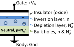
{{Image|MOS Capacitor.PNG|right|250px|Cross section of MOS capacitor showing charge layers}}
{{TOC|right}}
{{TOC|right}}
==MOS Capacitor==
==Schottky diode==
The '''MOS capacitor''' or '''metal-oxide semiconductor''' capacitor is a two terminal device consisting of three layers: a metal ''gate'' electrode, a separating insulator (often an oxide layer), and a semiconducting layer called the ''body''. The device operates using the [[field effect]], that is, the modulation of the surface conductivity of the semiconductor body by means of an applied voltage between the gate and the body.
 
==Operation==
{{Image|Seimiconductor band bending.PNG|right|350px|''Field effect'': Top panels: An applied voltage bends bands, depleting holes from surface (left). The charge inducing the bending is balanced by a layer of negative acceptor-ion charge (right). Bottom panel: A larger applied voltage further depletes holes but conduction band lowers enough in energy to populate an inversion layer.}}
A device based upon a uniformly doped ''p''-type body is described. The ''n''-type case is similar. The device has four regions of operation depending upon the applied voltage between gate and body:
#''Accumulation'': For a negative gate bias, holes are drawn to the semiconductor-insulator interface. A conducting surface extends from the bulk all the way to the interface, and the surface conductivity is enhanced by the accumulation of holes at the interface. 
#''Flat bands'': For a specific value of voltage, the bulk hole density is exactly the same from the bulk to the interface. The body is everywhere charge neutral because the hole density exactly balances the acceptor density. The ''flatband voltage'' corresponds to a zero potential drop in the body, but that does not necessarily correspond to zero applied voltage because of the [[contact potential]] between the metal gate and the body that leads to band bending even when zero voltage is applied.
#''Depletion'': For a positive gate voltage, the holes are pushed away from the positive charge on the gate electrode, and a surface layer depleted of holes is formed extending from the interface to the depth necessary to make the exposed, immobile, negative acceptor ion charge exactly balance the positive charge on the gate. Increase in positive charge on the gate with increasing voltage is balanced by expansion of the depletion layer, increasing the acceptor charge.
#''Inversion'': For positive gate voltages above a ''threshold voltage'', a surface inversion layer of electrons forms in a narrow layer near the interface. This conducting inversion layer is separated form the ''p''-type neutral bulk by the intervening insulating depletion layer of immobile acceptor charge. Once the gate voltage increases beyond the threshold voltage, additional positive charge on the gate is compensated by increased inversion layer electron charge, and the depletion layer depth no longer expands.<ref name=Tsividis>
 
Some authors subdivide the inversion regime into ''strong'', ''moderate'' and ''weak'' inversion. In strong inversion there is negligible depletion layer response and the inversion layer controls changes in the potential, while in weak inversion the potential still is controlled by the dopants and the inversion layer adapts. The moderate inversion regime is in between these two. See {{cite book |author=Yannis Tsividis, Colin McAndrew |title=Operation and modeling of the MOS transistor |edition=3rd ed |year=2010 |publisher=Oxford University Press |isbn=0195170156 |url=http://books.google.com/books?id=oYmYPwAACAAJ }}
 
</ref>
 
These various operation regions all are subsumed under the notion of the [[field effect]], the modulation of conductivity by an applied electric field. The figure illustrates the charge balance for the cases of depletion (top panels) and inversion (bottom panels). On the left side of the figure, the band edges are plotted as a function of depth into the capacitor. The electron population of the bands depends upon how close they are to the [[Fermi function#Fermi level|Fermi level]] (the horizontal dashed line): because this separation varies with depth, so does the occupancy of the bands. For example, the valence bands are bent far below the Fermi level near the interface, so the energy levels in the valence band near the interface are filled with electrons, and there are no holes. At greater depth from the interface, however, the valence band edge becomes the bulk value, and is close enough to the Fermi level to allow some electron vacancies (holes, in other words) in the valence band. Consequently there are holes present in the bulk region, which are of a density equal to that of the negatively charged acceptor impurities in this region, resulting in a neutral bulk. The right panels in the figure illustrate the charge densities as a function of depth that are a consequence of the band bending.
 
===Contact potential===
The flat band condition is examined further here, to explain why a zero applied voltage does not necessarily imply flat bands. The metal gate contains electrons, as does the semiconductor body. For this discussion, the insulator is imagined as a charge-free inert layer. Suppose an electron is taken from the metal and transferred to the semiconductor. There are three possibilities: no work is done, some work is done to transfer the electron, or the electron provides energy during the transfer. In the first case, zero applied voltage corresponds to flat bands, but in the other two cases a short circuit between metal and semiconductor leads to a net transfer of electrons making the gate negatively charged in the first case and the semiconductor in the second case. That is, without any applied voltage, a charge transfer occurs, and this transfer results in a potential difference at zero applied voltage, the ''contact potential''. Thus, to achieve flat bands (zero potential drop across the semiconductor), a ''flatband voltage'' is necessary.
 
The underlying cause of this charge transfer at a microscopic level is complicated in detail by the effects of interfaces including interface traps, and by charges in the insulating layer related to various defects. Within a few lattice spacings of an interface (≈1nm, say), the atomic arrangement differs from the bulk materials on either side of an interface, and the chemistry associated with such distortion can lead to charge dipoles (and related potentials) near this interface, even if the junction is free from defects. Two consequences are that the amount of charge transfer between the materials may depend upon the crystal orientation of the surfaces forming the interfaces, and it is not dictated entirely by the behavior of the metal and semiconductor idealized as bulk media. However, the driving force at an atomic level is the ability of some atoms to strip electrons from other atoms of a different species, a phenomenon called [[electronegativity]] of the atoms.<ref name=electronegativity>
 
See, for example, {{cite book |title=Silicon Materials Science and Technology X, Issue 2 |editor=Howard R. Huff, H. Iwai, H. Richter, eds |author=Hisham Z Massoud |url=http://books.google.com/books?id=KqIa5SCP93sC&pg=PA195 |pages=pp. 195 ''ff'' |chapter=Growth kinetics and electrical properties of ultrathin silicon-dioxide layers |isbn=156677439X |publisher=The Electrochemical Society |edition=Tenth symposium on silicon material science and technology |year=2006}}
 
</ref>
 
===Admittance===
{{Image|MOS equivqlent circuit.PNG|right|250px|Small-signal equivalent circuit of the MOS capacitor in inversion with a single trap level.}}
The MOS capacitor is often used as a test structure to monitor various fabrication steps in semiconductor processing. A key to these applications is the ''small-signal'' response of this device, that is, the current that flows in a circuit connecting this device to a small-amplitude gate voltage variation superposed upon a steady bias voltage. The ratio of the alternating current to the alternating voltage is the small-signal admittance of the device, and contained in this admittance is information about interface quality (traps, for example), insulator thickness, the distribution of dopants in the semiconductor body, and information on the defects in the semiconductor itself.
 
The basic ideas behind its use can be understood using the equivalent circuit in the figure. The circuit elements are:
:The oxide capacitance ''C<sub>OX</sub>''
:The depletion layer capacitance ''C<sub>D</sub>''
:The inversion layer capacitance ''C<sub>I</sub>''
:The trap capacitance ''C<sub>T</sub>''
:The trap conductance for holes ''G<sub>p</sub>''
:The trap conductance for electrons ''G<sub>n</sub>''
 
Based upon this circuit, the device small-signal admittance of only the semiconductor portion is given by:
:<math>Y_s =\frac { j\omega C_D + G_p\left( j\omega (C_I+C_T)G_n+j\omega C_I\ j\omega C_T \right)} {j \omega (C_I+C_T)G_n +j\omega C_I G_p +G_n G_p +j\omega C_I \ j\omega C_T} \ .</math>
 
The device admittance must include the series oxide capacitance. This result can be simplified in various bias regimes. For example, the depletion mode of operation is used for investigating doping profiles, and depends essentially upon ''C<sub>D</sub>''. Likewise, the behavior of interface traps is most readily captured through the three trap components ''C<sub>T</sub>'', ''G<sub>p</sub>'', and ''G<sub>n</sub>''.  The behavior of these various elements is described next.
 
====Depletion layer capacitance====
In depletion, the inversion layer is unimportant, and ''C<sub>I</sub>'' is not significant. The depletion layer capacitance can then be used to determine the distribution of dopant ions in the depletion layer, using two measurements of the MOS  capacitance: one at high enough frequencies that the traps cannot respond, and one at low enough frequencies that they have an equilibrium response. By comparing these two measurements, the distortion due to the traps can be corrected, and the doping profile can be determined. The connection between the depletion layer capacitance and the doping profile is found intuitively from the requirement for charge neutrality: if the gate charge is increased an amount ''ΔQ'', then the depletion width must expand to balance this charge. That is,
:<math> \Delta Q = q N_A(w) \Delta w \ , </math>
where ''w'' is the depletion width at the steady bias voltage and ''Δw'' is the incremental increase in the depletion width in response to ''ΔQ''. It is easy to measure ''Δw'' because the depletion layer capacitance is simply the parallel plate capacitance of the depletion layer (we use per unit area values):
:<math> C_D = \frac {\kappa_S \epsilon_0}{w} \ , </math>
where ''κ<sub>S</sub>'' is the dielectric permittivity of the semiconductor. Thus, if we extract ''C<sub>D</sub>'' from the measurement, the change in ''C<sub>D</sub>'' under a small-signal change in bias ''dV'' is a direct measure of the doping concentration at the depletion edge ''N<sub>A</sub>(w)'':
:<math>\frac{d}{dV} \frac {1}{C_D} = \frac{d}{dV} \frac{w}{\kappa_S \epsilon_0} = \frac {1}{\kappa_S \epsilon_0} \frac{dw}{dV} =\frac{1} {N_A(w)} \frac {1}{q\kappa_S \epsilon_0}\frac{dQ}{dV} \ , </math>
and it remains only to connect ''dQ/dV'' to the measured capacitance using the equivalent circuit. Assuming the traps do not play a role (or are corrected for):
:<math> \frac{dQ}{dV} = \frac{C_{OX} C_D}{C_{OX} +C_D} \ . </math>
Further details are left to the general references.
 
====Inversion layer capacitance====
{{Image|MOS CV curves.PNG|right|250px|Three types of MOS capacitance ''vs.'' voltage curves. ''HF''&nbsp;<nowiki>=</nowiki>&nbsp;high frequency, ''LF''&nbsp;<nowiki>=</nowiki>&nbsp;low frequency, ''V<sub>TH</sub>''&nbsp;<nowiki>=</nowiki>&nbsp;threshold voltage and ''V<sub>FB</sub>''&nbsp;<nowiki>=</nowiki>&nbsp;flatband&nbsp;voltage}}
The figure shows three different types of small-signal capacitance ''vs.'' voltage curves observed in the MOS capacitor, in this case on a ''p''-type substrate. A small-signal gate bias variation is superposed upon the steady bias ''V<sub>G</sub>''.  For steady voltages ''V<sub>G</sub>'' above the threshold voltage ''V<sub>TH</sub>'' an inversion layer can form. The inversion regime of biases is divided in the figure into the strong inversion regime, where the inversion layer capacitance is so large at low frequencies that the overall capacitance is close to the insulator capacitance ''C<sub>OX</sub>'' and the regime labeled simply "inversion", which is the regime where the inversion layer is gaining dominance over the depletion layer capacitance. These matters are explained further below.
 
The inversion layer becomes important for gate biases above the threshold voltage, and well below threshold the inversion layer capacitance is not important to the equivalent circuit. Also, in the MOS capacitor the inversion layer response to a small-signal change in gate bias is frequency dependent: an increase in gate bias demands a electrons to increase the population of the inversion layer. These electrons, however, are supplied by generation ''via'' traps in the depletion layer, and typically this generation is slow at temperatures up to room temperature.<ref name=MOSFET>
 
The electron response required by the inversion layer in the MOSFET is supplied by the source and drain contacts above threshold, not by generation-recombination, and is very much faster than in the MOS capacitor.
 
 
</ref> Thus, at high frequencies, the inversion layer will not respond, and the inversion layer capacitance is of minor importance in the equivalent circuit.
 
Thus, at low frequencies when the inversion layer fully responds to the small-signal gate bias, the ''low-frequency'' capacitance curve is:
:<math>\frac{dQ}{dV} = \frac{C_{OX} (C_D+C_I)}{C_{OX}+C_D+C_I} \ , </math>
the so-called ''low-frequency CV curve'', and when the small-signal gate bias is at a high frequency where the inversion layer does not respond at all:
:<math>\frac{dQ}{dV} = \frac{C_{OX} C_D}{C_{OX}+C_D} \ , </math>
the so-called ''high-frequency CV curve''. The slow response of the inversion layer means that the steady bias must be changed slowly so the inversion layer has time to accommodate. If instead the steady bias is ramped up rapidly from flatbands to inversion, the inversion layer will not form and the small-signal voltage will continue to follow the high-frequency CV curve (labeled "fast sweep" in the figure). The result is the so-called ''deep depletion CV curve''.
 
====Traps====
The above description of CV curves incomplete until the voltage dependence of the capacitance is found. That is accomplished by determining how the band bending in the semiconductor is related to the applied bias. The charge in the device can be written:
 
:<math>Q = Q_{SC}(\psi_S) + Q_{T}(\psi_S ) \ , </math>
 
where ''Q<sub>SC</sub>'' is the semiconductor charge and ''Q<sub>T</sub>'' is the trapped charge, both of which depend upon the band bending or potential drop ''&psi;<sub>S</sub>'' across the semiconductor, assuming the traps are at the interface. The total charge ''Q'' can be related to the field in the insulator, assuming no charge in the insulator, using [[Gauss's law]]:
:<math>Q = \kappa_{OX} \varepsilon_0 \frac{V_G-\psi_S}{t_{OX}} \ , </math>
where ''&kappa;<sub>OX</sub>'' is the dielectric permittivity of the oxide (about 3.9 for SiO<sub>2</sub>) and ''t<sub>OX</sub>'' is the thickness.
 
A change in gate voltage then alters the charge on the device as:
 
:<math>dQ = C_{OX}\left(dV_G - d\psi_S \right) = \left ( \frac {dQ_{SC}}{d \psi_S} + \frac {dQ_T}{d\psi_S} \right) d\psi_S = \left( C_{SC} + C_T \right)d\psi_S \ , </math>
where ''C<sub>T</sub> is the trap capacitance:
:<math>\frac {dQ_T}{d \psi_S} = C_T \ , </math>
and ''C<sub>SC</sub>'' is the semiconductor capacitance:
:<math>\frac {dQ_{SC}}{d \psi_S} = C_{SC} \ . </math>
Thus,
:<math>\frac{d\psi_S}{dV_G} = \frac {C_{OX}}{C_{OX}+C_T+C_{SC}} \ . </math>
The function ''Q<sub>SC</sub>'' can be calculated once the dopant distribution (the ''profile'') is known, either by calculation or measurement. However, the trap charge is available only by measurement, as it depends on details of interface chemistry that are not well understood, and cannot be deduced from a theoretical model. It is clear that the trap charge in ''Q'' will alter the dependence of ''&psi;<sub>S</sub>'' upon ''V<sub>G</sub>'', resulting in a larger change of bias necessary for a given change in ''&psi;<sub>S</sub>'' ( a so-called ''interface trap stretch-out''). At the same time, assuming a frequency small enough that the traps can respond, the device capacitance is affected by the traps:
:<math>\frac{dQ}{dV_G} = \frac {dQ}{dV_G} = \frac{dQ}{d\psi_S}\frac{d\psi_S}{dV_G}= \frac{C_{OX}\left(C_{SC} + C_{T}\right)}{C_{OX}+C_{SC} + C_{T}} \ , </math>
 
At high enough small-signal frequencies, the traps do not respond:
:<math>\frac{dQ}{dV_G} = \frac{C_{OX}C_{SC}}{C_{OX}+ C_{T}} \ . </math>
A comparison of capacitance at a low and a high frequency therefore allows determination of the trap capacitance, and enables empirical correction of the measurements for stretch-out.
 
The traps themselves can be studied by careful extraction of the trap conductance parameters as a function of frequency. Such measurements have shown that MOS devices do not have just a single trap level, but a range of interface traps distributed in energy across the band gap and located close to the semiconductor-insulator interface.
 
It may be noted that the MOS capacitor also can be used to study bulk traps in the semiconductor, and to study ion transport in the oxide layer (for example, the level of sodium contamination).


==Notes==
==Notes==
<references/>
<references/>

Revision as of 16:27, 21 January 2011

(PD) Image: John R. Brews
Cross section of MOS capacitor showing charge layers

Schottky diode

Notes