File:Seimiconductor band bending.PNG: Difference between revisions
imported>John R. Brews ({{Image_Details|user-pd |description = Band bending under external field for p-type semiconductor |author = ~~~ |date-created = 2011-01-06 |pub-country = |notes = Top panel: Applied voltage depletes holes from surface Bottom panel: Larger applied voltage further depletes holes but conduction band becomes low enough in energy to populate an inversion layer |versions = }}) |
imported>John R. Brews No edit summary |
||
| Line 4: | Line 4: | ||
|author = [[User:John R. Brews|John R. Brews]] | |author = [[User:John R. Brews|John R. Brews]] | ||
|date-created = 2011-01-06 | |date-created = 2011-01-06 | ||
|pub-country = | |pub-country = USA | ||
|notes = Top panel: Applied voltage depletes holes from surface Bottom panel: Larger applied voltage further depletes holes but conduction band becomes low enough in energy to populate an inversion layer | |notes = Top panel: Applied voltage depletes holes from surface Bottom panel: Larger applied voltage further depletes holes but conduction band becomes low enough in energy to populate an inversion layer | ||
|versions = | |versions = | ||
Revision as of 16:08, 6 January 2011
Summary
| Title / Description
|
Band bending under external field for p-type semiconductor |
|---|---|
| Citizendium author
|
John R. Brews |
| Date created
|
2011-01-06 |
| Country of first publication
|
USA |
| Notes
|
Top panel: Applied voltage depletes holes from surface Bottom panel: Larger applied voltage further depletes holes but conduction band becomes low enough in energy to populate an inversion layer |
| Other versions
|
If there are other versions of this media on CZ, please list them here. |
| Using this image on CZ
|
Copy the code below to add this image to a Citizendium article, changing the size, alignment, and caption as necessary.
|
Please send email to manager A T citizendium.org .
Licensing/Copyright status
This media, Seimiconductor band bending.PNG, is licenced under the Creative Commons CC0 1.0 Universal License
No copyright:
The person who associated a work with this licence waives all rights to the work under copyright law and all related or neighboring legal rights in the work, to the extent allowable by law.
Patent or trademark rights, or rights other persons may have either in the work itself or in how the work is used such as publicity or privacy rights, are not affected.
Read the full licence.
File history
Click on a date/time to view the file as it appeared at that time.
| Date/Time | Thumbnail | Dimensions | User | Comment | |
|---|---|---|---|---|---|
| current | 19:52, 11 March 2022 | 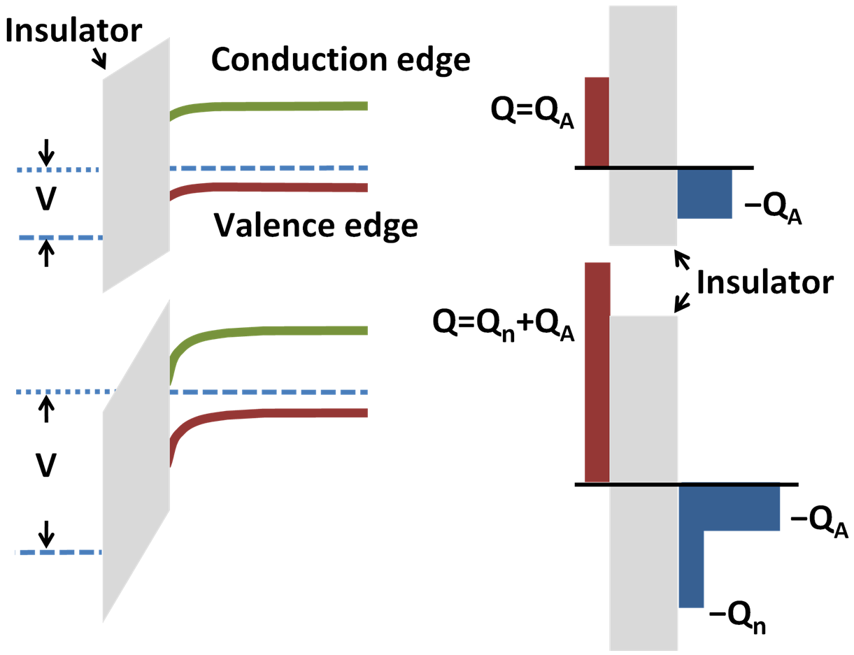 | 1,221 × 937 (88 KB) | Maintenance script (talk | contribs) | == Summary == Importing file |
You cannot overwrite this file.
File usage
The following 5 pages use this file: